Quality Commitment
JLCPCB takes every effort to improve our products, services and processes to meet or exceed our customers’ expectations. To promise customers the highest quality products and services, our quality commitment policy is driven by continuous improvement in product innovation, proactively pursue quality and reliability, and increase customers’ overall satisfaction.
Quality Control
Our goal are high-quality products and satisfied clients; therefore, quality control is an important part of our production process.
Quality assurance is implemented in every aspect, including:
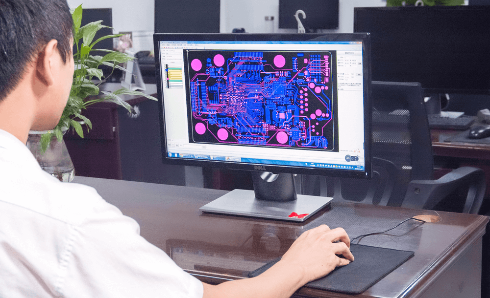
Every order submitted on JLCPCB, Gerber files will be reviewed by engineers before sent to production. Engineers will confirm design remaining true on the tolerance restrictions for board edge clearance, drill holes and spacing between pads, traces, etc. When engineers find problems in files, the system will send notice to customers' order list center and email, where customers can check this in time to avoid delay of production.
Ensuring maximum quality control of raw materials is one of the most basic tenets of product manufacturing in the PCB industry. JLCPCB has always been partnering with Industry-leading suppliers. We use top-level materials, like Nanya FR4 material, Solder mask with TAIYO INK PSR-2000; Lead-Free HASL-Rosh surface finish using upgraded raw materials which contain tin bars with silver.
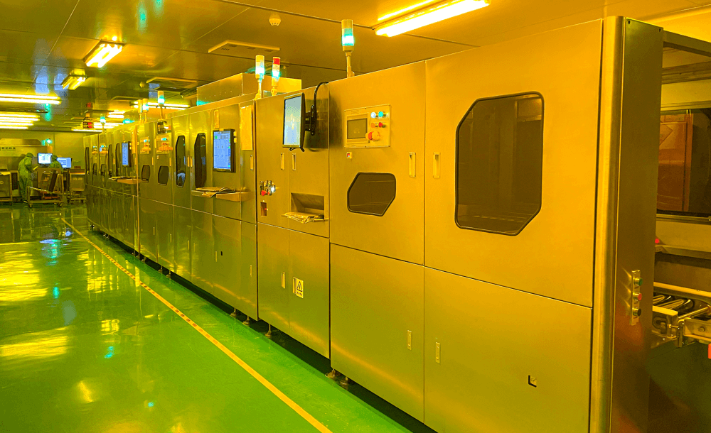
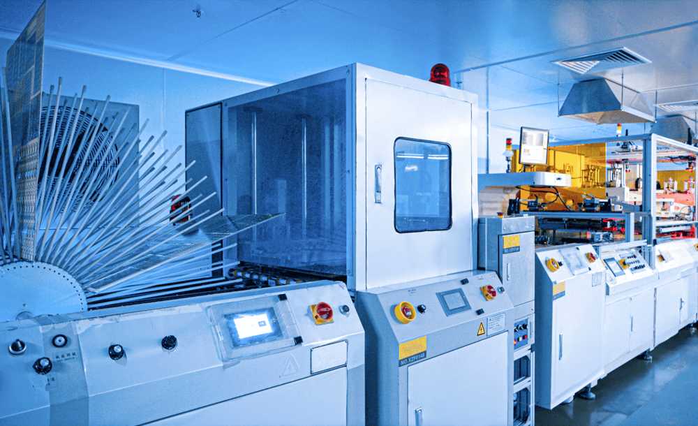
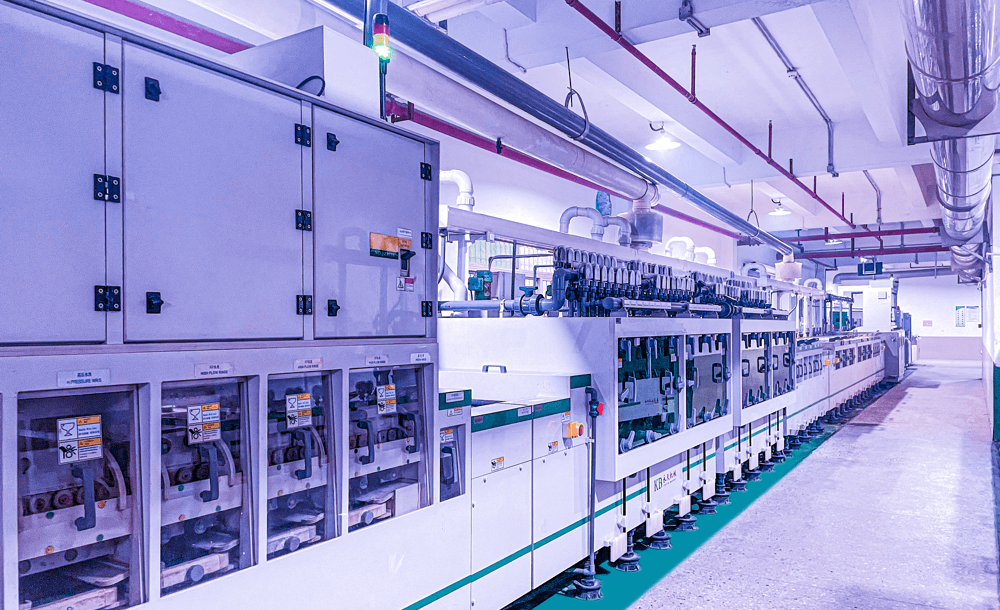
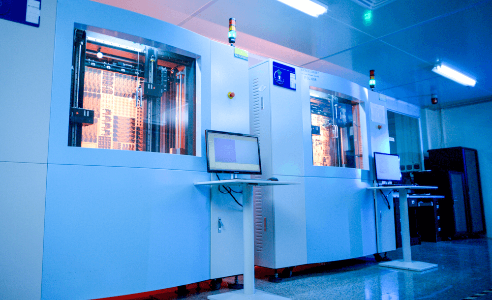
To ensure the best quality and reliability of PCB products, JLCPCB constants investments in advanced equipments including:
● Fully-automatic LDI exposure Machines.
● Fully-automatic Solder mask Production lines.
● Fully-automatic PCB Test Machines.
● Fully-automatic CCD exposure Machines.
● Fully-automatic PCB Etching Equipments.
● Fully-automatic Screen-printing Production lines.
● Fully-automatic Electroplating lines.


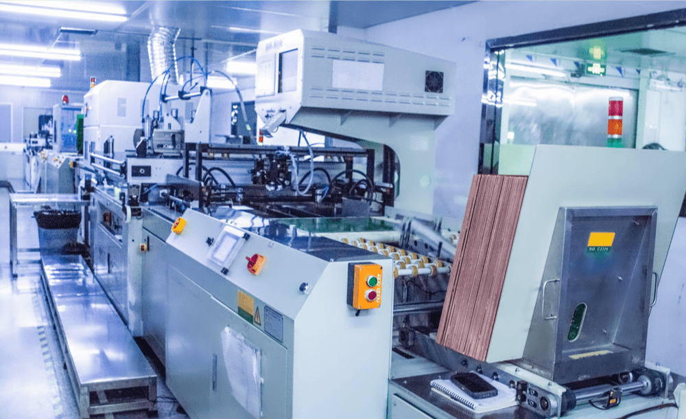
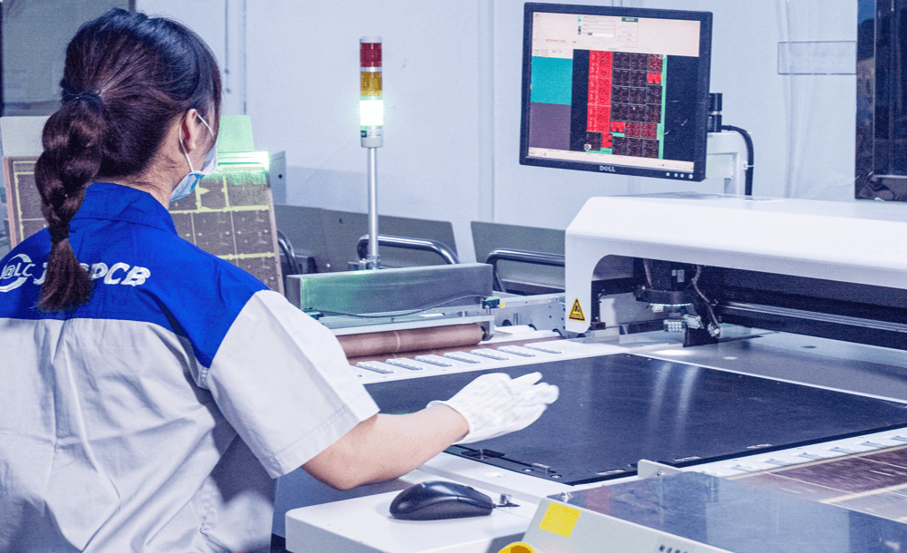
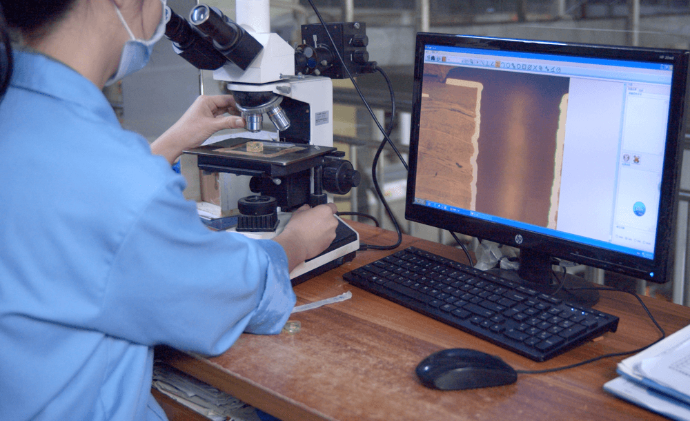
AOI testing after Pattern Plating. It is the automated visual inspection of PCB in which a camera is used to scan the board in extremely fine detail to check for any defects or failures. It is applied after Hot Air Solder Leveling.
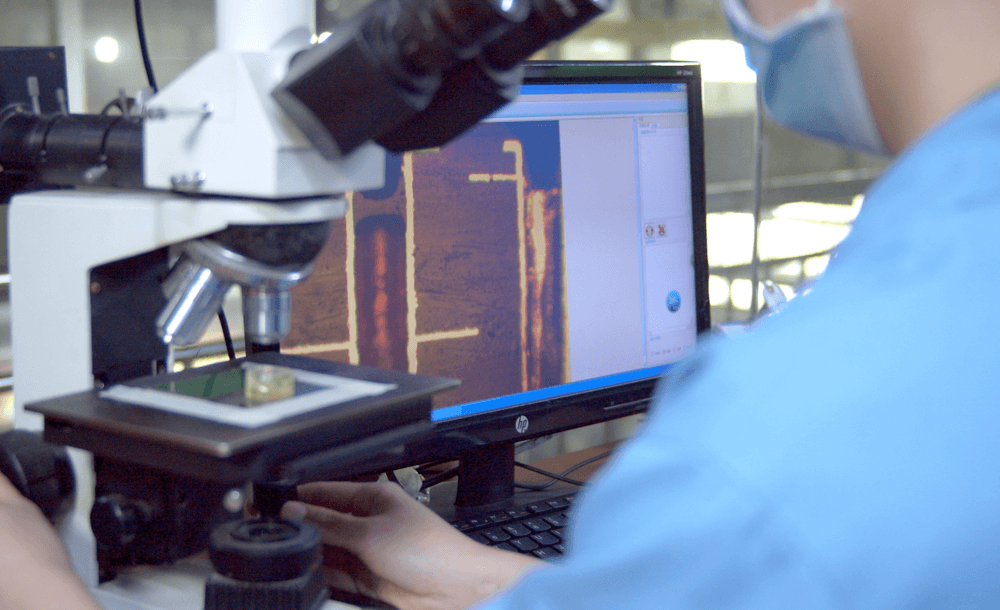
This electric testing uses electro-mechanically controlled probes to access parts on the board, similar to ICT. The precision movement can probe points on PLCCs, SOICs, PGAs, SSOPs, QFPs and others.

Smart system and powerful data center help staffs to track the reason and operator easily when PCB occurred an error in production. No matter he is an engineer reviewing gerber files, a worker or a leader working in which production workshop, need to undertake the responsibility if he indeed made the mistake.
Certifications
JLCPCB works hard to obtain, maintain, and uphold the highest standards. The following certificates granted to us confirmed that we are consistently providing the utmost quality products and services to our customers.
